This Is the World's Largest Computer Chip
- Cerebras Systems, a Silicon Valley startup in stealth mode since 2016, has released the world's largest functional computer chip.
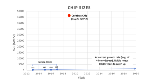
- At 56 times the size of the next largest chip, the company says its chip's computing power will enable artificial intelligencesolutions at an exponentially faster rate.
- The chip has a redundant structure, meaning that the expected imperfections in chip manufacturing will be insignificant.
The optics of computer chip design and manufacturing are central to whatever device you're reading this article on, but chips have never really been considered sexy. The most love they've gotten is in the name Silicon Valley itself, which refers to silicon, the semiconductor material inside the chips.
ADVERTISEMENT - CONTINUE READING BELOW
Then again, a computer chip has never been both functionally viable and the size of a brand-new iPad—until now.
In a smartphone, a chip is usually about the size of your fingernail in a smartphone or, on the larger side of the scale, the size of a postage stamp. But Cerebas Systems, a Los Altos, California-based startup that has been in stealth mode since 2016, just released the world's largest computer chip.
How large? Try 8.5 inches on each side and 1.2 trillion transistors inside, all working hard to allow your computer to complete complex tasks. A typical computer chip, by contrast, merely has millions (or occasionally billions) of transistors switching between binary states of 0 and 1, the language of computers.
So what does that mean for you? Andrew Feldman, CEO and cofounder of Cerebras Systems, tells Popular Mechanics that the rate of research and development in the artificial intelligence space will be immensely expedited. While AI already powers many aspects of our lives—for Feldman's grandmother, he says, that comes down to asking Alexa to play Frank Sinatra songs—the full potential has been stymied by hardware that's just too slow.
ADVERTISEMENT - CONTINUE READING BELOW
"The chip is a similar solution to AI as a minivan is a solution to having three kids," Feldman says. "What we saw were characteristics of the AI world. And what the software wanted the hardware to do was very difficult."
The Big Chip's Early Flops and Failures

ADVERTISEMENT - CONTINUE READING BELOW
Historically, there have been major hurdles to producing mammoth computer chips like the one Feldman and his team of over 200 are designing, manufacturing, and, yes, selling.
Renowned computer scientists already took a stab at it back in the 1980s. “Some of the most famous engineering folks tried and they failed spectacularly,” Feldman says.
Take Trilogy Systems, a computer company founded in 1980. Led by Gene Amdahl, his son Carl Amdahl, and Clifford Madden, the team wanted to create a super advanced semiconductor manufacturing technique.
At the time, the elder Amdahl was flush with cash from his successful company, Amdahl Corporation. The firm quickly raised $230 million for the new venture, making it the most well-funded startup company in Silicon Valley up to that point.
ADVERTISEMENT - CONTINUE READING BELOW
The plan was to create an unprecedented semiconductor manufacturing technique to help build an IBM-compatible mainframe computer that was cheaper and more powerful than existing systems (accordingly, a similar goal to what Feldman envisions).
Trilogy came up with an idea that included wafer scale integration, a rarely used system of building integrated circuit networks that use up an entire silicon wafer to produce just one super-chip. The team wanted to produce a computer chip that was 2.5 inches on each side (at the time, only chips of about 1/4 inch per side could be reliably manufactured at scale).
Alas, the company's semiconductor fabrication plant was damaged during construction by a winter storm; the chip's design wasn't sufficient for reasonable manufacturing yields; and the chip's interconnecting technology couldn't be reliably manufactured, as layers tended to delaminate, and at the time there wasn't an automated way to repair soldering errors.
ADVERTISEMENT - CONTINUE READING BELOW
 Nerds Creating More Powerful Semiconductors
 Researchers Make Computer Chips 250x Faster
 IBM Announces 5 Nanometer Semiconductors
Morale was plummeting by 1984 when The New York Times covered Trilogy's internal turmoil and technical difficulties. The younger Amdahl left the company in June 1984. His account of his times at Trilogy follow:
"It's not like we made mistakes, it's just that we didn't know enough about the issues we would face,'' he said in a recent telephone interview. ''It got so complicated that you could put the smartest people in the world on the project and they would give you gut feel rather than fact. There just wasn't an appreciation of how hard it was going to be,'' he added. ''I would wake up in the middle of the night in cold sweats, thinking about what we were doing wrong. All I was dreaming about was the computer design and how the pieces fit together. I would dream schematic diagrams of the machine.''
ADVERTISEMENT - CONTINUE READING BELOW
By mid-1984, the firm said it was too difficult to manufacture its computer design. Gene Amdahl stepped down as CEO. Prior to the dot-com bubble and burst in 2001, Trilogy was known as one of the greatest financial flops in Silicon Valley's history.
Feldman, of course, is looking to take a different and, hopefully more successful, path.
“We realized we had an opportunity to solve the problem very differently than [they] had tried and created a real opportunity for us,” he said.
The Cookie Dough Design Process
ADVERTISEMENT - CONTINUE READING BELOW
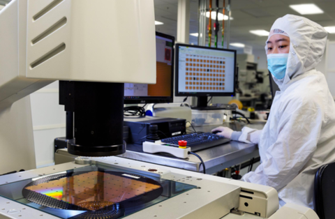
All chip design comes down to virtually the same process called photolithography. Here's how it works: There is equipment that manufactures chips and prints them out of circular wafers of pure silicon. Typically, that means placing a grid of as many chips as possible onto the wafer and then slicing up the wafer to create separate chips.
This is how transistors are etched onto the surface of the silicon wafer. But Cerebras uses the whole wafer for its chips, rather than slicing and dicing chips out from the silicon.
Let's use a cookie analogy, because we're hungry. The equipment that manufacturers chips prints them out like a wafer, or "like a big piece of cookie dough," says Feldman. Then, the chips are punched out. But you know that leftover dough in between the cut-outs, which you can mush together to get three or four more cookies out of it? Well, Feldman took that idea to the chip.
ADVERTISEMENT - CONTINUE READING BELOW
“We decided, holy cow, we can use the entire piece of dough," he says. The team would find a way to use as much of the wafer as possible.
All in all, it took about 3.5 years to finally perfect the system. So it's a good thing the company had at least $112 million in venture capital funding to play with.
AI Computing's Crazy Demand
Deep learning, a type of artificial intelligence that teaches computers how to do what humans can naturally—learn by example—must be fed a large set of labeled data and neural network architectures to train the system.
ADVERTISEMENT - CONTINUE READING BELOW
So yes, it's profoundly computationally intensive.
A recent report by OpenAI, a San Francisco-based artificial intelligence research center, showed that between 2012 and 2018, the computing power used to train the largest models increased by 300,000 times.
In short, AI computing demand is doubling every 3.5 months, according to a Cerebras white paper.
So far, the GPU (graphics processing system) has become the mainstay chip for AI work. That's the same kind of chip that runs your PlayStation or Xbox, not to mention these computationally intensive neural networks. But it's no longer powerful enough, Feldman says.
GPUs are made up of lots of little communicating cores performing little computations that communicate together, he explains. "By putting them on separate chips, the industry has made communication very expensive. It’s time consuming, it’s slow, it’s power hungry.”
ADVERTISEMENT - CONTINUE READING BELOW
But what if you put all of these communication cores on one chip, rather than hundreds or thousands? All on the same silicon strip?
“The big limitation in artificial intelligence is that it takes weeks or months to test a single idea," Feldman says, due to hardware that's just too slow for the software. “What if instead, in that month, you could test 1,000 ideas?"
Cerebras claims its chip packs 400,000 tiny AI optimized cores, which allow the chip to contain an entire neural network, rather than spreading the data out over multiple GPUs, using a bunch of connecting cords in a giant tangle of a mess.
All in all, this system takes up less power and less space if you're willing to pay for the upfront investment. Feldman would not disclose the cost for the Cerebras system, but says the aim is to save customers from what they would pay with their current setup.
ADVERTISEMENT - CONTINUE READING BELOW
Feldman says whole data center systems at governments, financial institutions, and more—his ideal customers—could set up this new system in about an hour, without impacting anything on the software side.
“It’s complexity of data, plus the characteristics of that complexity,” he says. “Sometimes it might be hard to move a big boulder, other times it may be hard to move a huge number of little pebbles. They have different characteristics. AI requires a new type of truck to move it, and that’s the new type of computing.”
The Chip's Technical Challenges
ADVERTISEMENT - CONTINUE READING BELOW
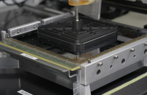
That little smidge of bonus dough after you've cut out your cookies is analogous to what's left over when cutting chips from silicon. The challenge: How do you create one giant cookie, rather than 100 little cookies with wasted space in between? It had never effectively been done, Feldman says.
Of course, manufacturing has its flaws. When the silicon wafers are cut into tiny pieces to create chips, there are always a few that turn out imperfect.
“The bigger the chip, the more likely it costs more" if you have to toss one, Feldman says. “We invented a technique to withstand flaws rather than require flawless wafers.”
Imagine you have a Tic-Tac-Toe board, but rather than it being 3-by-3 squares, it's 600-by-600. That makes about 360,000 total squares. Now imagine you took one extra row across the top and one extra row down the side and added that into your board.
ADVERTISEMENT - CONTINUE READING BELOW
"If there was a flaw in the middle, you used the spare from these extra rows you just added" to ensure the giant chip is still usable, Feldman says. He calls this the "redundancy scheme."
Feldman's ultimate goal is to increase the speed of productivity in the AI space so that we can dramatically change our lives. We'll have autonomous car fleets sooner, be able to employ 5G wireless communication applications with ease, and smart cities will flourish.
But for that to happen, that massive computing power looming in the background and minding its own business must be the most important guy in the room.
“In a new world where everything has to work together … the faster the communication, the faster the innovation," Feldman says.


